


World’s Smallest Atom-memory Unit Created?!?! Deets Inside…..
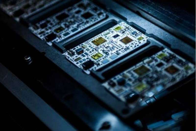
The smallest memory device yet has been developed by researchers, a development that can lead to quicker, smaller, and more energy-efficient electronic chips for consumer electronics and brain-inspired computing. Scientists at the University of Texas at Austin in the US have also discovered the physics for these compact devices that activate dense memory storage capabilities. In the study recently published in the journal Nature Nanotechnology, the researchers decreased the size of what was then the thinnest memory storage unit, decreasing the area of the cross section to a single square nanometer. According to the researchers, having a handle on the physics on these devices that pack dense memory storage capacity allowed them to make the device much smaller. They said the ultra-small holes in the material provide the secret to unlocking the capability of storing high-density memory.
Deji Akinwande, a co-author of the report explained: "When a single additional metal atom goes into that nanoscale hole and fills it it confers some of its conductivity into the material, and this leads to a change or memory effect," The researchers claim that the discovery could apply to hundreds of similar atomically thin materials, although they used the compound molybdenum disulfide—also known as MoS2—as the primary nanomaterial in their analysis. Smaller processors enable manufacturers to produce more compact computers and phones, they said, adding that their energy demands are also reduced and performance is increased by shrinking chips. The scientists clarified that this means quicker and smarter equipment that needs less power to run.
At that time the original unit called the "atomristor" by the researchers, was the thinnest memory storage device ever recorded, with a single atomic thickness layer. Shrinking the memory chip, however, is not only about making it thinner, they added, but also designing it with a smaller cross-sectional area. "The scientific holy grail for scaling is going down to a level where the memory function is controlled by a single atom, and this is what we achieved in the new study." The new system falls under the memoristor group, a field of memory research based on electrical components capable of manipulating the resistance between its two terminals without the need for a third terminal in the centre. These can be smaller than currently used memory cards, according to the researchers, and boast more storage space. They said the new memristor offers a capacity of about 25 terabits per square centimetre, which, compared to currently available flash memory devices, is about 100 times higher in memory density per layer.
TAGGED :